

Why are processors square or rectangular? The answer lies in production efficiency and packaging
Although silicon wafers are circular, processor chips are mostly cut into squares or rectangles. The reasons behind this are cost, efficiency, and packaging.



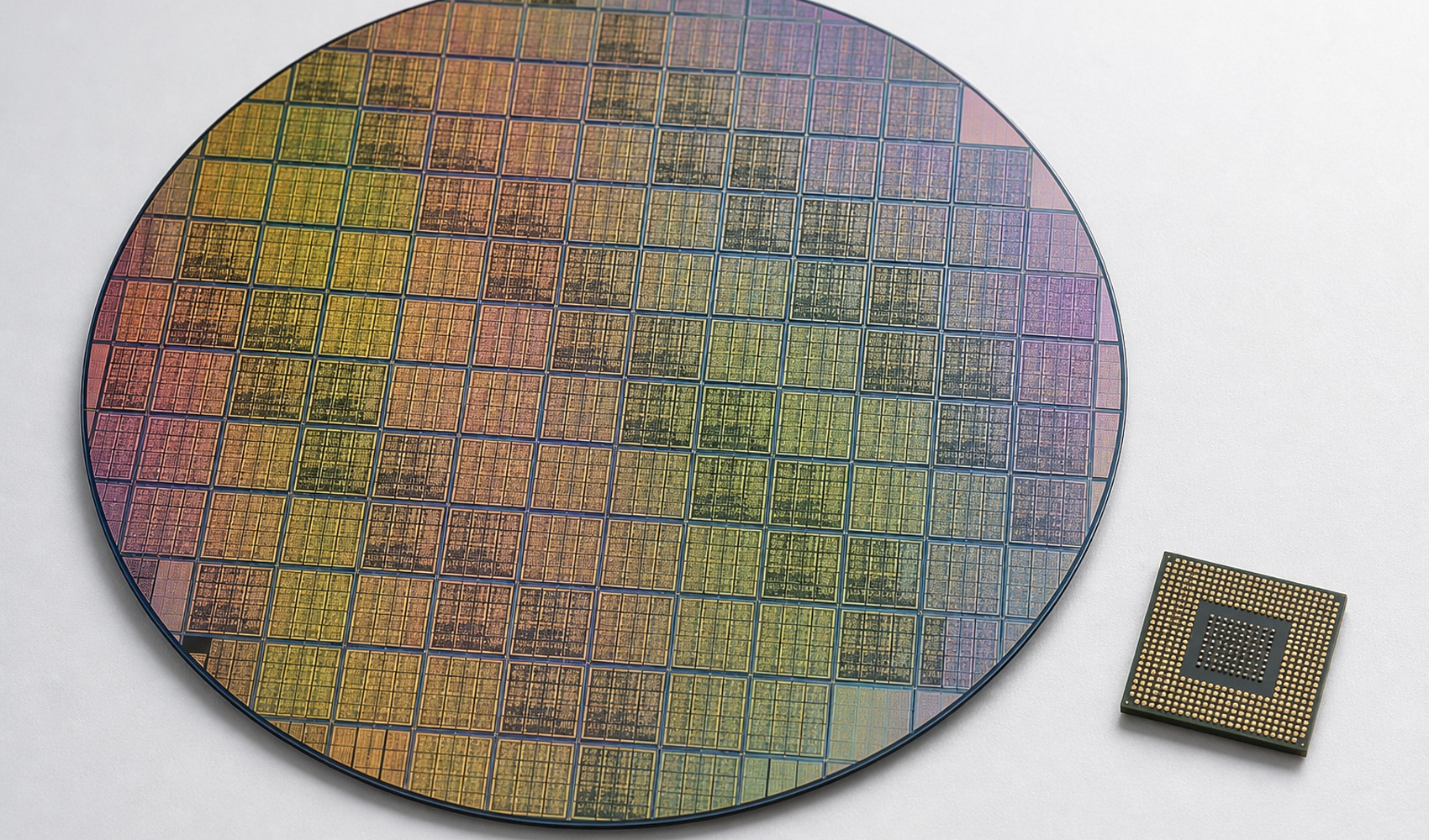
Most of the processors used in computers and phones appear square or rectangular from the outside. However, the silicon wafers from which these chips are produced are circular. According to technical information provided by Webtekno, this situation is less about a design habit and more about the efficiency, cutting, and packaging requirements of semiconductor manufacturing.
The handheld outer package of a processor is not the same thing as the silicon chip that performs the actual calculations. The large metal surface seen on desktop processors is often part of the heat spreader and protective package. Beneath this, there are one or more small silicon dies. These dies form the actual processor structure, which contains billions of transistors and connection layers.
PRODUCTION BEGINS WITH A ROUND WAFER
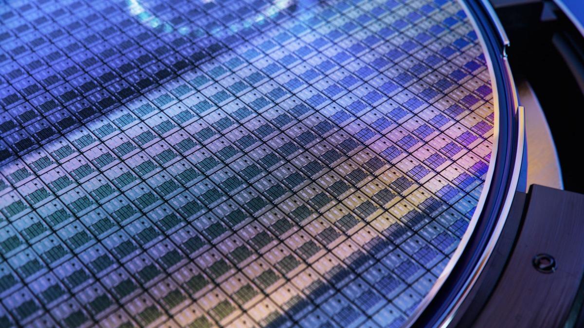
The reason wafers are round stems from the production method of silicon crystals. High-purity silicon is grown into a single-crystal cylindrical ingot. When this cylindrical structure is cut into very thin slices, circular wafers emerge. In current semiconductor manufacturing, 300-millimeter diameter wafers are widely used.
Instead of placing a single giant processor on this round surface, the manufacturer creates many copies of the same design. After stages such as photolithography, numerous dies arranged side-by-side appear on the wafer. The square and rectangular shape allows these dies to be placed in regular rows and columns.
The most important advantage of this arrangement is seen in the cutting process. When production is complete, the chips on the wafer are separated from each other through a process called "dicing." Straight-edged square or rectangular dies can be separated more easily along straight cutting lines. With round chips, both the cutting becomes more complex and unused silicon gaps are created around each chip.
ROUND CHIPS ARE POSSIBLE BUT NOT EFFICIENT
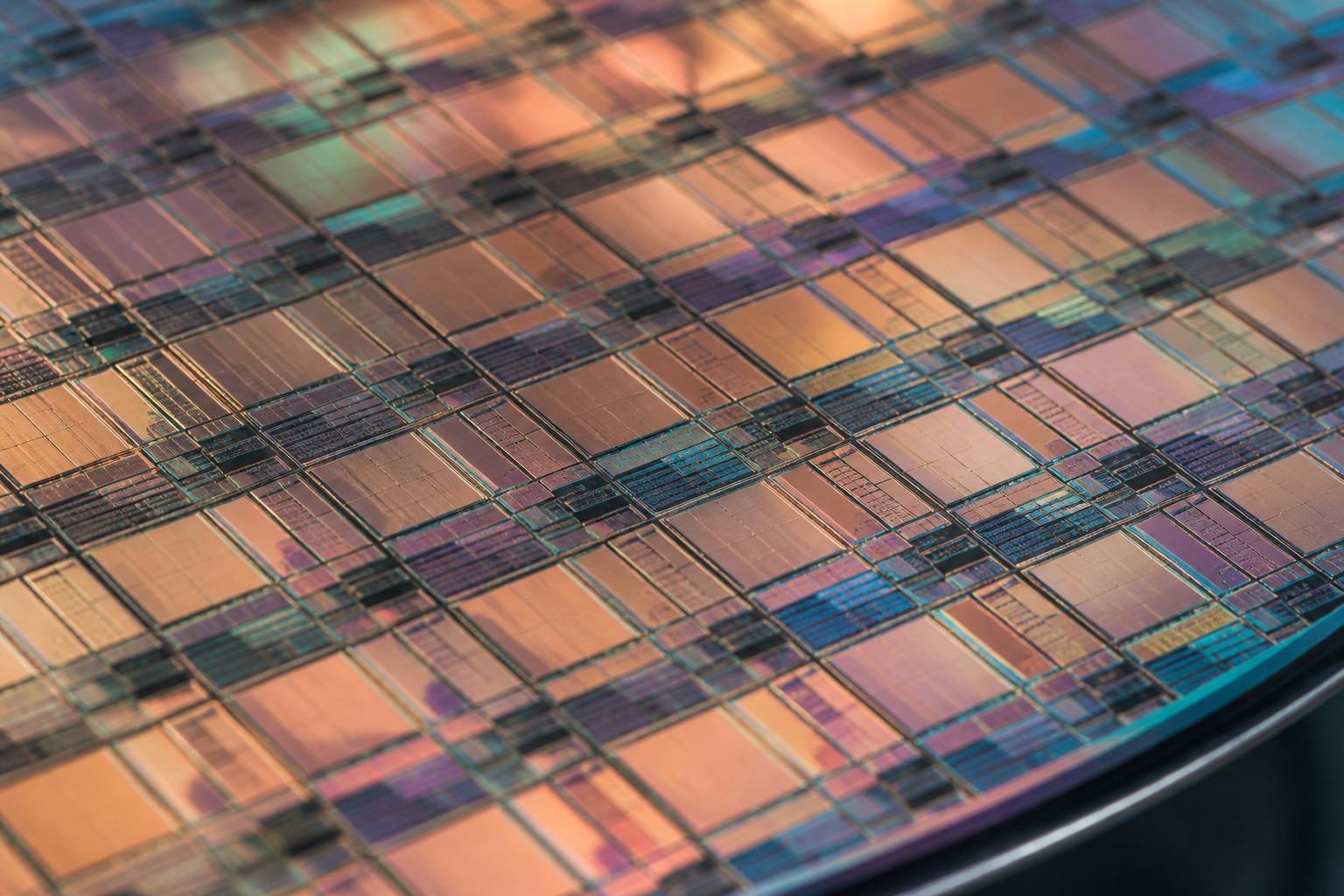
Technically, it is not physically impossible to produce a round silicon chip. However, there is no significant advantage to this in mass production. A significant portion of the cost in semiconductor manufacturing is linked to how efficiently the wafer area is used. The more working chips obtained from a wafer, the higher the production yield.
When round chips are placed side-by-side, there are inevitable gaps between them. These gaps mean unused silicon area. Furthermore, tracing and cutting circular boundaries individually can create a more complex and costly process compared to straight cutting lines. For this reason, a four-cornered structure offers a more practical solution for the manufacturer.
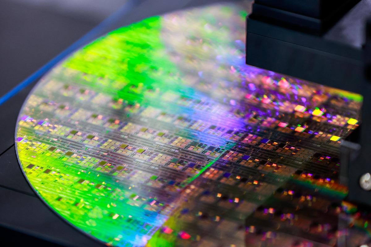
It is not accurate to say that all components inside a processor are square. Modern processors consist of transistors, cache blocks, CPU cores, memory controllers, input/output units, and connection layers. The geometry of these structures can vary depending on the production technology and design requirements.
Nevertheless, a square or rectangular workspace provides significant convenience from an engineering perspective. Design tools can place circuit blocks more regularly within these boundaries; variables such as signal paths, power distribution, heat density, and manufacturability can be calculated simultaneously.
PACKAGING, COOLING, AND THE CHIPLET EFFECT
Once the silicon die is produced, it is not connected directly to the motherboard. It goes through a packaging stage for transporting electrical connections to the outside world, mechanical protection, and heat transfer. The large metal cover seen on desktop processors spreads the heat generated by the processor over a wider surface, facilitating contact with the cooler.
Flat and four-cornered packages can also be placed more regularly with other components on printed circuit boards. The size of these packages is not determined solely by the area of the silicon inside; socket design, the number of contact points, power requirements, and cooling needs are also taken into account.
In recent years, the chiplet approach has also become widespread in processor architecture. In some designs, such as in AMD's current desktop and server processors, CPU cores and input/output units can be produced as separate chips and combined within the same package. Intel also uses multiple processing units in the same package with advanced packaging methods in its various products.
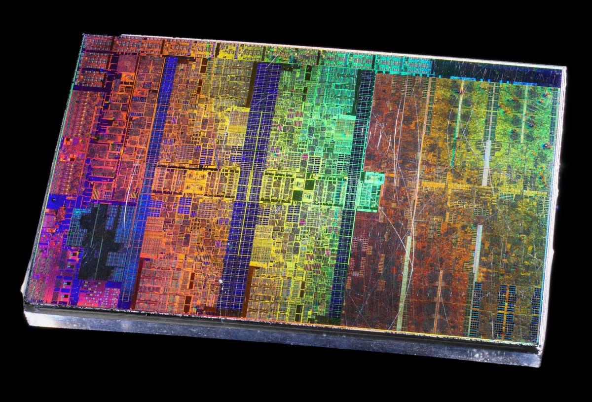
Chiplet design has not eliminated the square or rectangular appearance of processors from the outside. On the contrary, multiple four-cornered chips can be found side-by-side under a single package or on different layers using advanced packaging methods. This approach can offer the opportunity to increase yield with smaller parts instead of producing a single very large chip.
In the future, 2.5D and 3D packaging, memory solutions closer to the processor, and the combination of different production technologies in the same package may become more common. However, in the current production chain, the square and rectangular form continues to be one of the most practical options in terms of wafer efficiency, ease of cutting, circuit layout, packaging, and cooling.
News Source: 12punto
Most Read

Enver Altaylı arrested in Kaşif Kozinoğlu investigation

I am facing an atmosphere as if Kozinoğlu’s killer has been found

Lieutenants at the Courthouse

Notable moments from Erdoğan's UN speech

Our economy is resilient to shocks and the investment environment has been strengthened

Will the Yemen tender fall to Turkey?

Armed attack on a school in Manisa: 11 students injured, 2 in critical condition

A distant election? The symbiotic life of two countries

Do we have to buy a phone?

First appearance by Ali Koç in a long time